Gallium Arsenide
CMK manufactures Semi-insulating and Semiconducting Gallium Arsenide wafers and ingots by LEC (Liquid Encapsulated Czochralsky) or VGF (Vertical Gradient Freeze) growth method. Required electrical parameters are achieved through high purity 6N input material (Gallium and Arsenic). In order to attain the chosen level of concentration, the dopants like Zinc, Silicon and Tellurium are used.
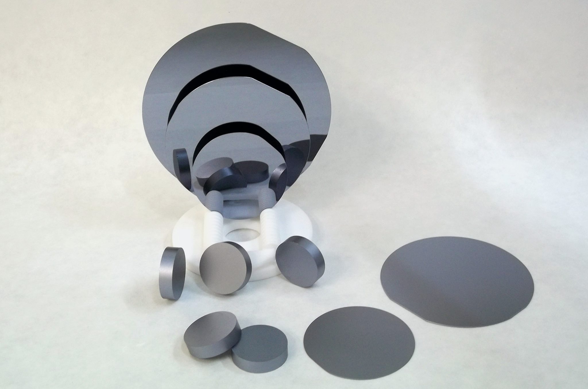
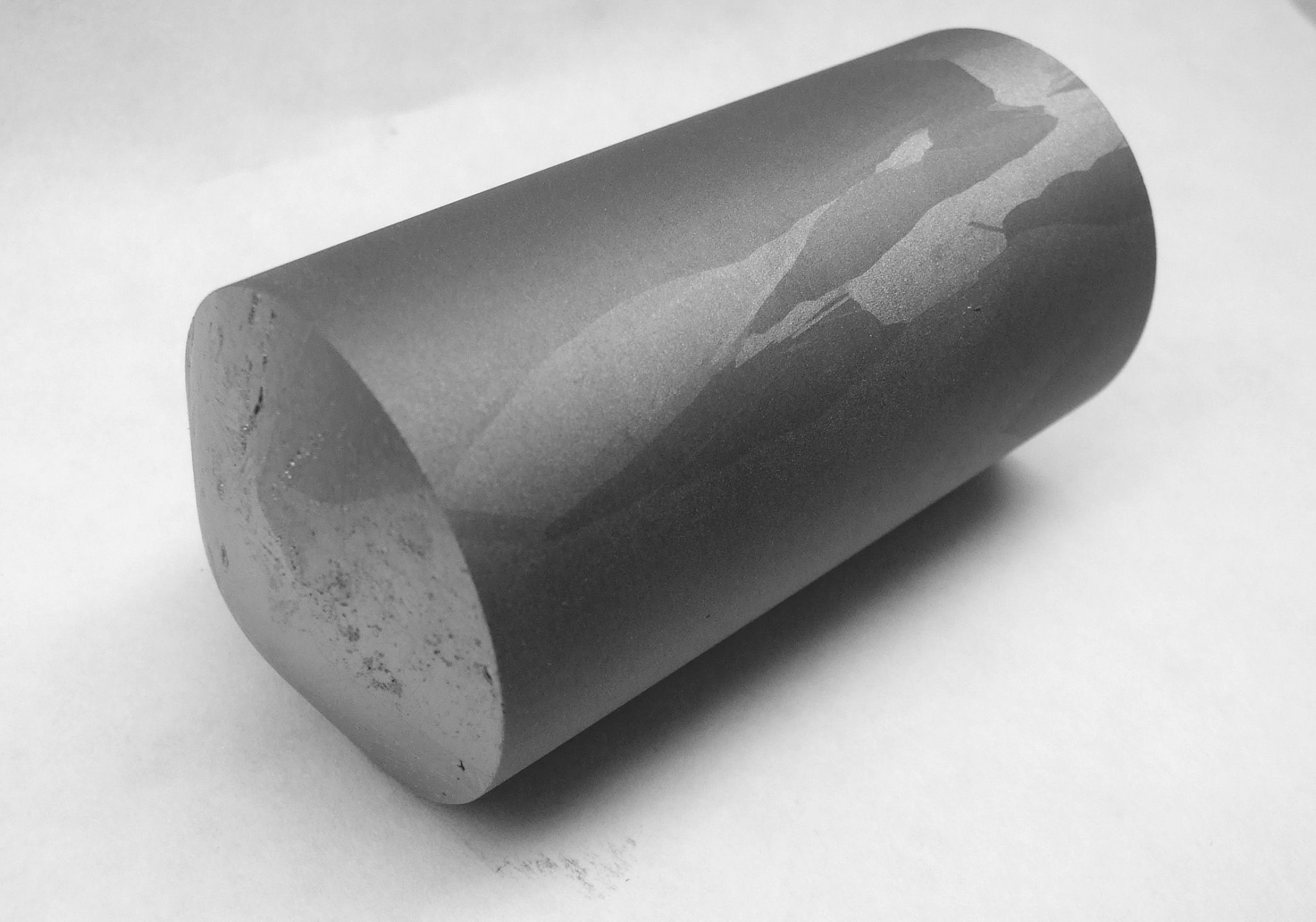
The production process involves growing of monocrystalline and polycrystalline Gallium Arsenide in PBN and High purity quartz crucibles. We offer monocrystalline wafers and whole ingots with diameter from 2” up to 4“ with quality suitable for epitaxial processing and high-frequency and optoelectronic applications.
High quality material is produced by trained fully qualified staff to meet customer’s often specific needs.
| Specification of monocrystalline Gallium Arsenide |
| GaAs semi-insulating, undoped | GaAs semiconducting, p-type & n-type |
| Diameter | wafers: from 2“ up to 4“ ingots & synthesis: from 2“ up to 6“ |
| Thickness | wafers: from 325 um up to 750 um ingots & synthesis: from 2“ up to 6“ |
| Dopant | – | Zinc, Silicon, Tellurium |
| Carrier concentration | – | n-type 1 x 10¹⁶ – 2 x 1018 cm-3 p-type 1 x 10¹⁶ – 5 x 1019 cm-3 |
| Crystal orientation | (100), (110), (111) |
| Off orientation | up to 15°, if necessary >15° |
| Resistivity | >1 x 10⁷ Ωcm | >1 x 10⁻³ Ωcm |
| Hall mobility | >6000 cm2 V-1s-1 | n-type 1 x 10¹⁶ – 2 x 1018 cm-3 p-type 1 x 10¹⁶ – 5 x 1019 cm-3 |
| Etch pit density (EPD) | <1 x 104 cm-2 | LEC: <7 x 104 cm-2 VGF: <5 x 103 cm-2 |
| Surface treatment | wafers: as cut/lapped/etched/single & double side polished ingots and synthesis: as ground/as grown/as cut |
| Flat orientation | US SEMI or EJ standard |
| Packaging | Standard/Empak/Fluoroware/Fluoroware sealed with N2 |
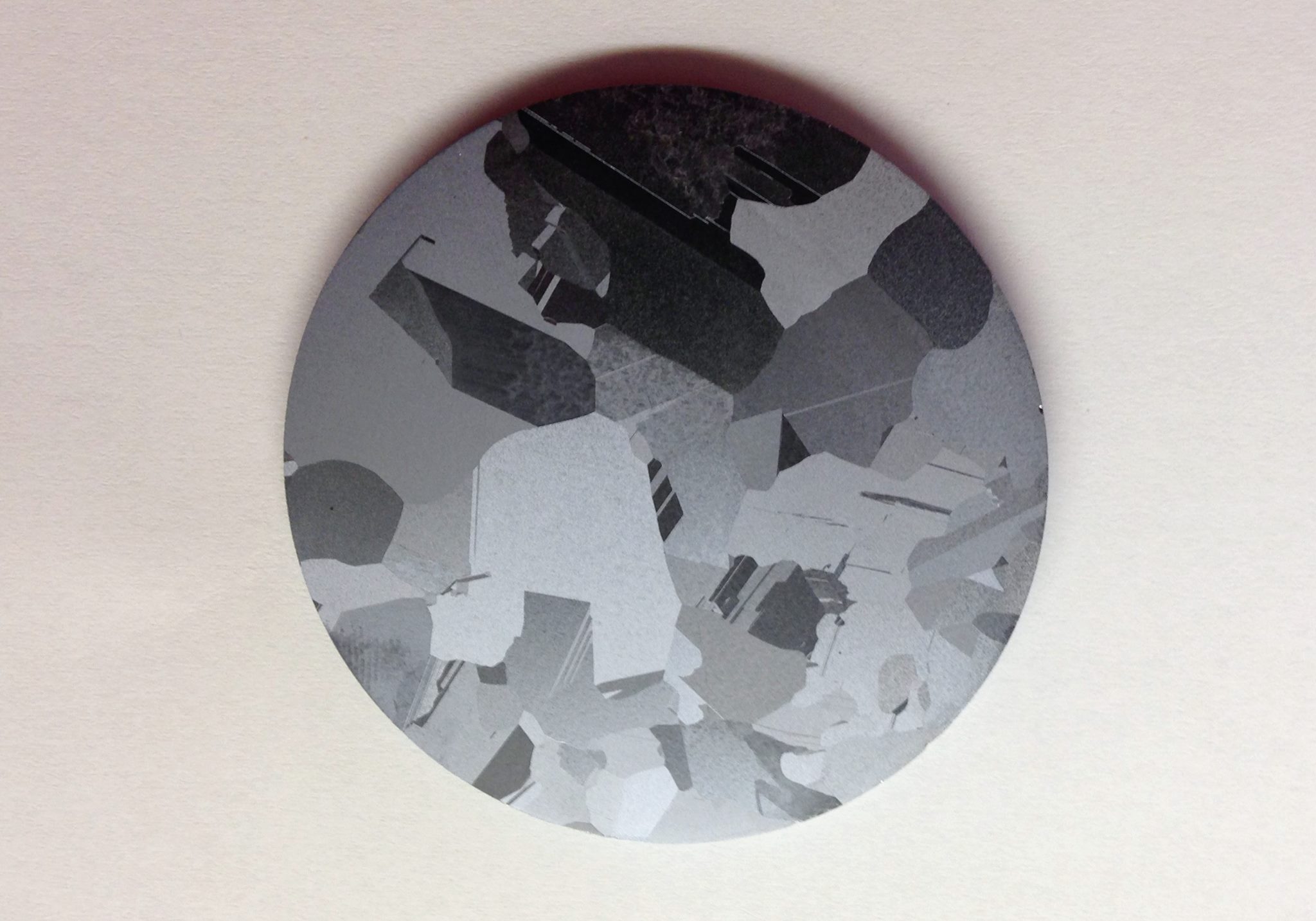
Furthermore, we offer polycrystalline Gallium Arsenide with diameter from 0.5“ up to 4.25“ in the form of wafers and ingots. Our products are manufactured under high pressure with precise stoichiometry control of high purity input material. Each ingot is analyzed using GDMS with the aim to determine the level of its purity.
Polycrystalline Gallium Arsenide is used as an input material for further processing and applications.
| Specification of polycrystalline Gallium Arsenide |
| GaAs semi-insulating, undoped | GaAs semiconducting, p-type & n-type |
| Diameter | wafers: from 0.5“ up to 4.25“ ingots & synthesis: from 2“ up to 6“ |
| Thickness | wafers: from 0.5 mm up to 40 mm ingots & synthesis: from 50mm up to 100mm |
| Dopant | – | Zinc, Silicon, Tellurium |
| Carrier concentration | – | n-type 1 x 10¹⁶ – 2 x 1018 cm-3 p-type 1 x 10¹⁶ – 5 x 1019 cm-3 |
| Resistivity | >1 x 10⁷ Ωcm | >1 x 10⁻³ Ωcm |
| Hall mobility | >1 x 103 cm2 V-1s-1 | n-type >1500 cm2 V-1 s-1 p-type low |
| Etch pit density (EPD) | <1 x 104 cm-2 | LEC: <7 x 104 cm-2 VGF: <5 x 103 cm-2 |
| Surface treatment | wafers: as cut/etched ingots and synthesis: as ground/as grown/as cut |
| Flat orientation | US SEMI or EJ standard |
| Packaging | Standard/Fluoroware/Fluoroware sealed with N2 |
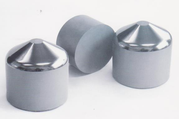
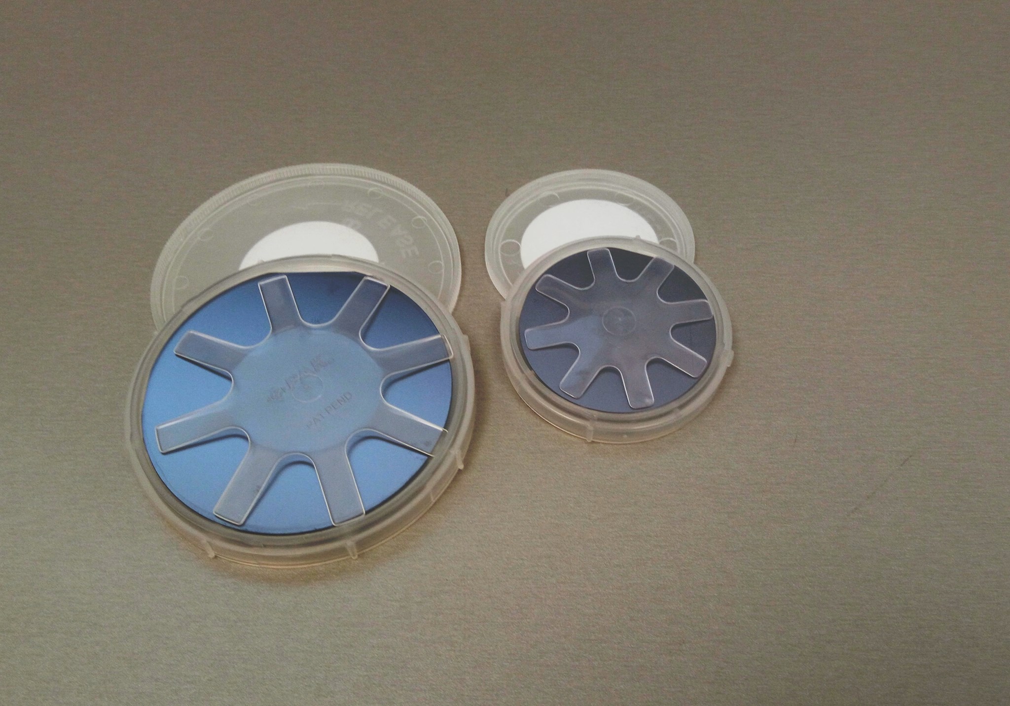
Packaging used for GaAs material
We offer various types of packaging suitable for as cut as well as polished wafers:
- Fluoroware individual container,
- Fluoroware type tray individually sealed in inert atmosphere,
- Empak type 25 wafers box,
- Standard type suitable for packaging of whole ingots and crystals;

Gallium Arsenide field of application
Monocrystalline GaAs
Semi-insulating GaAs
- diameter: 2, 3 and 4 inch wafers & ingots
- SI undoped
Semiconducting GaAs
- diameter: 2, 3 and 4 inch wafers & ingots
- SC n-type – Si and Te doped
- SC p-type – Zn doped

Application field: LED industry, High-tech industry, MEMS microelectromechanical systems, Solar products, Active components, Integrated circuits, Telecom parts, etc.
Polycrystalline GaAs
GaAs wafers
- diameter: 0.5 – 4.25 inch
- thickness: 0.5 mm – 40 mm
- SI undoped
- SC n-type Si and Te doped, p-type Zn doped
GaAs Ingots up to 6“ for VGF growing
- diameter: 4.5 – 6 inch
- thickness: 50 – 100 mm
- SI undoped
- SC n-type Si and Te doped, p-type Zn doped
- Growth method: LEC and VGF

Application field: Polycrystalline GaAs is used as a starting material for the manufacture of GaAs products (LED industry, Fiber optic communication, Microwave circuits, Solar cells application, High efficiency photovoltaic devices, etc.)
Blanks for Optical Components
Opto GaAs wafers
- diameter: 0.5 – 4.25 inch
- thickness: 1 mm – 20 mm
- SI undoped
- Growth method: LEC
Application field: Wireless communication, PHEMT technology, Opto-electronic components (Photodiodes, Phototransistors, Photoresistors, Integrated optical circuits, Optocoupler, Laser diodes, Infrared emitting diodes), Chips, Optical fiber communication, Solar products, etc.
© 2024 CMK Ltd.
Created by m@rtin